Intel-Technion Collaboration: New Lab Inaugurated
A laboratory for manufacturing processes in the semiconductor industry was inaugurated at the Wolfson Faculty of Chemical Engineering
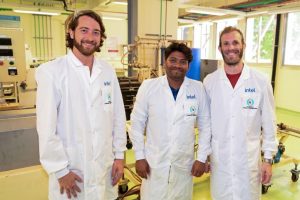
A laboratory for manufacturing processes in the semiconductor industry was recently inaugurated at the Wolfson Faculty of Chemical Engineering. Supported by Intel, the establishment of the laboratory was led by Prof. Yaron Paz along with the faculty’s teaching laboratories engineer, Ms. Luba Texler.
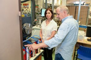
The inauguration was attended by Dr. Sigal Ben-Zvi, Intel-Technion Relations Manager, who cut the ribbon, and Esti Gazit, Academic Relations Coordinator at Intel Israel. The lab team showed the equipment and various workstations to the attendees.
“The microelectronics industry is essentially a chemical industry,” said Prof. Paz, “as it is a process industry that combines diverse chemical reactions, diffusion, and flow, all under controlled conditions. Therefore, it is not surprising that about 15% of the Faculty’s graduates integrate into this industry. For more than twenty years, the Faculty has been offering a course on the manufacturing processes of semiconductor devices, aimed not only at teaching these processes from a chemical engineer’s perspective but also at providing tools for integrating into this industry while creating a common language with professionals from various backgrounds and disciplines. Now, thanks to the new laboratory, we are adding another dimension to the training our graduates receive.”
The laboratory will allow faculty students to experience manufacturing processes similar to those used in the “real world” of the semiconductor industry: atomic layer deposition, silicon oxidation, wet etching, metal layer growth, and photolithography.
“Budget constraints forced us to be creative and to design and build some of the experimental stations ourselves and adapt the lab to work in a non-dust-free space,” said Prof. Paz. “It’s important to understand that the lab was built at a total cost of less than $250,000, a minimal amount compared to similar labs in the field. The main idea was to allow students to familiarize themselves with, understand, and operate most of the functional units existing in the microelectronics industry, while circumventing the requirement for miniaturization and its financial implications. Additionally, we ensured that the functional units we created had many degrees of freedom, allowing students to ‘play’ with the various variables and thereby verify (and confront) theories on the subject.”
“This laboratory is the highlight of the collaboration between Intel and the faculty,” said Dr. Sigal Ben-Zvi. “It is the first laboratory of its kind in the chemical engineering faculties in Israel, and it will provide students with real work experience and a very relevant set of tools for the industry.”


